Table of Contents >> Show >> Hide
- What Does “Factory Defect IC” Really Mean?
- Why Sandpaper Enters the Story
- Microsoldering: Where Nerves Go to Become Professionals
- How a Defective IC Can Be Diagnosed Before Repair
- The Repair Process: From Defect to Revival
- Important Tools for This Kind of IC Repair
- Risks of Reviving an IC This Way
- When This Repair Makes Senseand When It Does Not
- What This Repair Teaches About Electronics
- Extra Repair Experience: What It Feels Like to Revive a Factory Defect IC
- Conclusion
Every electronics repair bench has its own mythology. Some stories involve toasted capacitors, mysterious USB ports, or a laptop that “just stopped working” after meeting half a latte. But few repairs sound as wonderfully unhinged as this one: a factory defect IC revived with sandpaper and microsoldering. It sounds like the kind of sentence that makes engineers squint, hobbyists lean forward, and warranty departments quietly leave the room.
Yet the idea is not pure madness. In the world of board-level repair, especially when dealing with rare components, discontinued chips, prototype hardware, or “this must work tonight” situations, technicians sometimes go far beyond ordinary soldering. They scrape solder mask, rebuild pads, expose copper, run jumper wires thinner than a human hair, and inspect everything under a microscope like electronic surgeons with caffeine privileges.
This article explores how an integrated circuit with a factory defect can potentially be brought back to life using careful abrasion, precision cutting, and microsoldering. We will look at what can go wrong inside or around an IC, why sandpaper is both useful and dangerous, how microsoldering makes impossible-looking repairs possible, and what this kind of repair teaches us about electronics, patience, and the surprisingly dramatic life of tiny metal pads.
What Does “Factory Defect IC” Really Mean?
An IC, or integrated circuit, is a tiny electronic city. Inside that black package are semiconductor structures, metal interconnects, bond wires, pads, and protective materials designed to keep everything electrically connected and physically safe. When everything is manufactured correctly, the chip behaves like a quiet genius. When something goes wrong, it may act more like a toaster in a thunderstorm.
A factory defect IC can fail for several reasons. The problem might be a short between adjacent pads, a missing or damaged bond wire, contamination, misaligned packaging, cracked die material, poor plating, incorrect solder wetting, or even damage caused during assembly. Some defects are visible under magnification. Others hide until power is applied and the board behaves like it has developed trust issues.
In many cases, the sensible repair is replacement. Remove the bad IC, install a known-good part, verify operation, and go home feeling professional. But sometimes replacement is not practical. The chip might be obsolete, custom-programmed, locked, rare, expensive, or physically tied to the device’s identity. In those cases, repairers may attempt something more creative: exposing the problem area and manually restoring the connection.
Why Sandpaper Enters the Story
Sandpaper is not the first tool most people associate with microelectronics. It belongs in woodworking shops, auto body repair, and that one kitchen drawer full of mystery hardware. Still, controlled abrasion can be useful in electronics repair when the goal is to remove a small amount of protective coating, oxidation, epoxy, solder mask, or packaging material.
In a delicate IC repair, sandpaper may be used to gradually expose copper, internal pads, or the surface of a package. The key word is gradually. This is not “scrub until something shiny appears.” This is more like archaeology, except the artifact is smaller than a sesame seed and can be destroyed by one heroic sneeze.
Fine-grit sandpaper, abrasive film, fiberglass scratch pens, and precision blades are commonly used in board repair to expose traces or clean damaged areas. When done properly, abrasion creates access to a conductive surface that can accept solder. When done poorly, it removes the thing you were trying to save. That is the repair equivalent of rescuing a goldfish with a leaf blower.
The Difference Between Useful Abrasion and Disaster
Useful abrasion removes only the unwanted material. Disaster removes the pad, trace, bond wire, or die structure. A skilled technician works slowly, checks progress under magnification, cleans debris often, and stops as soon as enough conductive material is exposed. The goal is not beauty. The goal is electrical continuity without collateral damage.
For PCB pad repair, this same principle applies. If a solder pad lifts, burns, or disappears, the technician may scrape back solder mask from the connected trace, tin the exposed copper, then bridge the connection with a fine wire. On an IC-related repair, the scale is smaller and the risk is higher, but the logic is similar: expose, clean, tin, connect, support, and test.
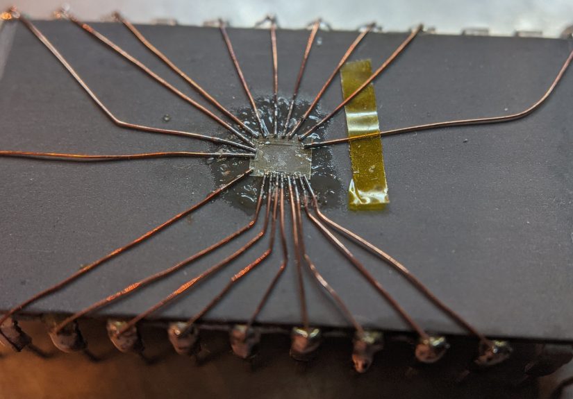
Microsoldering: Where Nerves Go to Become Professionals
Microsoldering is the art of soldering very small electronic components and connections under magnification. It is used in phone repair, console repair, laptop board repair, medical device service, data recovery, and advanced electronics restoration. It usually involves a microscope, fine soldering tips, hot air, quality flux, precision tweezers, thin solder, solder wick, and wire so tiny it looks like it was stolen from a spider’s craft drawer.
When reviving a defective IC, microsoldering may involve attaching a fine jumper wire from an exposed pad or trace to the correct board connection. It may also involve correcting a bridge, removing a short, rebuilding a pad, or reattaching a lead. The work demands controlled heat because ICs do not enjoy being cooked. Too little heat creates weak joints. Too much heat damages pads, nearby components, or the chip itself.
Why Flux Is the Unsung Hero
Flux deserves its own applause. It cleans oxidation, helps solder flow, reduces surface tension, and makes tiny joints behave less like stubborn glitter. Without flux, microsoldering can become a messy fight between heat, metal, and disappointment. With flux, solder tends to wet the exposed copper or component lead more evenly, allowing the technician to form a cleaner connection with less heat exposure.
Good microsoldering is not about dumping solder onto a problem. It is about using just enough solder to create a reliable electrical and mechanical joint. Excess solder can bridge adjacent pins, create shorts, or form blobs that look impressive but fail inspection. In this kind of repair, a shiny mountain is not a victory. A tiny, smooth, well-wetted joint is.
How a Defective IC Can Be Diagnosed Before Repair
Before anyone touches sandpaper or a soldering iron, diagnosis matters. A repairer should confirm that the IC is actually the problem. Randomly sanding electronics is not troubleshooting; it is modern art with smoke.
The diagnostic process usually starts with visual inspection. Under a microscope, the technician looks for cracked solder joints, damaged pads, solder bridges, corrosion, missing components, lifted traces, or signs of heat stress. Then comes electrical testing. A multimeter can check resistance, continuity, shorts to ground, and whether power rails behave normally. In more advanced cases, an oscilloscope, thermal camera, current-limited bench power supply, or logic analyzer may be used.
One common clue is a short between pins or pads that should be isolated. Another is a missing signal where continuity should exist. If the IC has a visible manufacturing flaw, such as merged pads or a malformed bond area, the repairer may decide to physically access the defect and correct it.
Current Limiting Saves Boards
A current-limited power supply is one of the best friends a repair bench can have. It allows a device to be powered safely while limiting how much current can flow during a fault. If a defective IC is shorted, current limiting can prevent further destruction and help locate the problem. It is the electrical equivalent of saying, “Let’s not burn the house down while we investigate the toaster.”
The Repair Process: From Defect to Revival
Every repair is different, but a careful IC revival using sandpaper and microsoldering often follows a logical sequence. The process below is an educational overview, not a recommendation to attack valuable electronics without training. Tiny chips are not forgiving teachers.
1. Inspect and Map the Circuit
The technician identifies the IC, studies the board layout if available, and determines which pins or pads are involved. If schematics are unavailable, continuity testing can reveal where traces go. Photos should be taken before work begins, because once the repair starts, “I think it used to look like this” is not a reliable documentation strategy.
2. Protect Nearby Components
Kapton tape, heat shielding, and careful board positioning help protect nearby parts. Small resistors and capacitors can be blown away by hot air or accidentally nudged by tweezers. They are tiny, expensive breadcrumbs, and losing one can create a new mystery.
3. Remove Coating or Package Material Carefully
This is where fine abrasive tools come in. The goal may be to expose a damaged pad, reveal a hidden conductor, or remove material covering the defective area. The technician works slowly under magnification. Dust and debris are cleaned away with isopropyl alcohol and lint-free swabs. If the repair involves the IC package itself, extra caution is required because internal structures are fragile.
4. Clear the Defect
If the problem is a short caused by merged metal or contamination, a fine blade may be used to separate the connection. If the problem is an open circuit, the repairer prepares a place where a jumper wire can be soldered. The repair area must be clean, stable, and conductive enough to accept solder.
5. Tin the Exposed Area
A tiny amount of flux is applied, followed by a very small amount of solder. The purpose is to coat the exposed copper or metal pad so a jumper wire can attach. This step requires careful heat control. Too much heat can delaminate pads or damage the IC. Too little heat produces a dull, unreliable joint.
6. Add a Jumper Wire
Fine insulated wire, enamel wire, or micro coax may be used depending on the signal. The wire is positioned with tweezers and soldered to the exposed repair point. The other end connects to the correct pad, trace, via, or component lead. The wire should be routed to avoid stress, moving parts, sharp edges, and hot components.
7. Secure the Repair
Once the electrical connection is verified, the repair should be mechanically supported. UV mask, epoxy, or other suitable insulating material can secure the wire and prevent movement. A jumper that works on the bench but snaps during reassembly is not a repair; it is a cliffhanger.
8. Clean, Inspect, and Test
Flux residue is cleaned, the repair is inspected under magnification, and continuity is checked. The device is powered using current limiting before full operation is attempted. If the IC responds correctly, the technician can move from cautious optimism to the sacred repair phrase: “Well, that actually worked.”
Important Tools for This Kind of IC Repair
A successful factory defect IC repair depends heavily on tools. A basic soldering iron from a garage drawer may be fine for speaker wires, but microsoldering requires more precision.
Microscope or High-Quality Magnification
A stereo microscope gives depth perception and allows the repairer to see bridges, cracks, fibers, flux residue, and solder behavior. Many failures are invisible to the naked eye. Under magnification, however, a “mystery fault” can suddenly reveal itself as a solder bridge the size of a dust mite with a bad attitude.
Temperature-Controlled Soldering Station
Controlled heat is essential. A station with fine tips allows the technician to apply heat accurately without roasting the board. Different solder alloys require different temperatures, and lead-free solder often needs more heat than traditional tin-lead solder.
Hot Air Rework Station
Hot air is useful for removing and installing surface-mount ICs, reflowing solder, and warming the repair area. Airflow must be controlled because too much force can scatter nearby components. Nobody wants to finish an IC repair and then discover three capacitors have emigrated.
Flux, Solder Wick, and Fine Solder
Flux improves wetting. Solder wick removes excess solder. Fine solder gives better control. Together, they help the repairer avoid blobs, bridges, and thermal overwork.
ESD Protection
Electrostatic discharge can damage integrated circuits instantly or weaken them in ways that show up later. A grounded mat, wrist strap, ESD-safe tools, and proper handling practices are not optional decoration. They are cheap insurance against invisible damage.
Risks of Reviving an IC This Way
This kind of repair can be brilliant, but it is risky. Sanding an IC or PCB can create conductive debris. Cutting too deeply can sever internal structures. Heat can damage silicon, loosen nearby parts, or weaken adhesives. Jumper wires can change signal behavior if the circuit involves high speed, radio frequency, impedance control, or sensitive analog measurement.
There is also the issue of reliability. A revived IC may function perfectly on the bench, but long-term durability depends on the quality of the joint, mechanical support, thermal cycling, vibration, and the environment in which the device operates. A repair for a hobby project, vintage device, or one-off prototype may be acceptable. A repair for safety-critical equipment requires much stricter standards.
When This Repair Makes Senseand When It Does Not
Reviving a factory defect IC with sandpaper and microsoldering makes sense when the component is rare, irreplaceable, custom-programmed, or needed for data recovery. It may also make sense as an educational experiment or proof-of-concept repair.
It does not make sense when a replacement IC is cheap and available, when the board is safety-critical, when the defect affects unknown internal structures, or when the technician lacks the tools to inspect and verify the work. Sometimes the smartest repair is replacement. Other times, the smartest repair is admitting the board has joined the great recycling bin in the sky.
What This Repair Teaches About Electronics
The biggest lesson is that electronics repair is not only about replacing parts. It is about understanding how materials, current, heat, design, and manufacturing all interact. A factory defect IC may look like a tiny black rectangle, but it contains a story: how it was built, how it failed, and whether a patient human can persuade it to work again.
It also teaches respect for manufacturing tolerances. Modern integrated circuits are produced at astonishing scale and precision. Most work flawlessly. But when a tiny defect slips through, the consequences can be dramatic. One shorted pad or broken connection can stop an entire device. At that scale, a speck of contamination can become the villain.
Finally, this repair shows why skilled technicians are still valuable in an age of disposable electronics. Anyone can throw away a board. It takes knowledge, patience, and a slightly heroic tolerance for frustration to bring one back.
Extra Repair Experience: What It Feels Like to Revive a Factory Defect IC
Working on a factory defect IC is a strange mix of science, craft, and emotional negotiation. The first experience most technicians notice is how quickly confidence changes under a microscope. At normal desk distance, the board looks simple. Under magnification, it becomes a landscape of copper cliffs, solder hills, dust boulders, and suspicious shiny objects. That is when the repair stops being theoretical and becomes very real.
The most useful habit is slowing down. Beginners often want to solve the problem immediately: more heat, more solder, more pressure, more movement. Experienced repairers learn that “more” is usually the enemy. More heat lifts pads. More solder creates bridges. More pressure breaks traces. The winning move is often less: less solder, less force, less time on the joint, and more inspection between steps.
When sandpaper or abrasive film is involved, patience matters even more. A practical approach is to make a few gentle passes, clean the area, inspect it, and repeat. The moment usable metal appears, stop. It is tempting to keep polishing until the surface looks perfect, but electronics repair is not jewelry making. A slightly ugly exposed conductor that solders well is better than a beautiful crater where the pad used to be.
Another real-world lesson is that flux can make a repair look magical. A dry joint may refuse solder completely, causing the technician to suspect bad metal, wrong temperature, or personal failure. Add proper flux, and suddenly the solder flows exactly where it should. It feels like cheating, except it is just chemistry doing its job. The trick is cleaning afterward, because leftover flux can hide bridges, attract grime, or cause issues depending on the type used.
Jumper wire routing is another place where experience shows. A wire that is electrically correct can still be mechanically foolish. If it crosses a screw post, sits under a shield, bends sharply, or floats unsupported, it may fail later. A good repairer thinks about reassembly before celebrating. The best jumper wire is short, supported, insulated where needed, and placed where it will not be crushed, pulled, or cooked.
Testing is where optimism meets reality. The first continuity beep after a difficult repair feels fantastic, but it is only one checkpoint. The next steps are checking for shorts, powering with current limiting, watching current draw, confirming signal behavior, and testing the device in real use. A revived IC may pass the first test and fail the second. That is not defeat; it is information.
One of the most valuable experiences is learning when to stop. Not every IC can be saved. If the die is cracked, internal damage is extensive, or the repair requires connections that cannot be made reliably, continuing may waste time or destroy surrounding parts. Good repair work includes judgment. The goal is not to win a battle against physics. Physics has a very strong legal department.
Still, when the repair works, it is deeply satisfying. A device that was dead because of one tiny manufacturing flaw suddenly boots, powers up, reads data, or produces the signal it was meant to produce. That moment explains why microsoldering attracts patient tinkerers and professional repairers alike. It turns invisible problems into visible solutions, one carefully placed wire at a time.
Conclusion
A factory defect IC revived with sandpaper and microsoldering is more than a flashy repair story. It is a reminder that electronics are physical objects, not magic slabs of silicon. Pads can short. Traces can break. Coatings can hide useful conductors. With careful diagnosis, controlled abrasion, proper flux, precise soldering, and patient testing, even a seemingly doomed IC may have one more chance to do its job.
This kind of repair is not for every board or every technician. It demands magnification, steady hands, ESD awareness, heat control, and the humility to stop before making things worse. But in the right situation, it can save rare hardware, recover important data, preserve vintage electronics, or simply prove that a tiny factory flaw does not always get the final word.